What happens when technology hits a literal wall of fire? The digital age is currently colliding with the strict physical limits of thermodynamics. Data centers rely on massive server farms that generate crippling heat while struggling to pack computing power into shrinking spaces. Faster processors create vicious cycles of energy consumption required just to keep the machines cool. The tech industry desperately needs a breakthrough to prevent global computing from burning itself out.
• Data centers face extreme heat and space limitations.
• Faster processors generate unmanageable thermal output.
• The industry needs new thermal solutions to sustain growth.
Researchers in Japan engineered a radical solution processing data at unimaginable speeds without thermal overload. They developed a nonvolatile switching element handling information in just forty picoseconds. This is one thousand times faster than standard chips. The device relies on ultrathin layers of tantalum and manganese-tin manipulated by ultrafast light pulses. This bypasses the friction causing overheating in standard silicon processing.
• A Japanese device processes data in forty picoseconds.
• The element is a thousand times faster than standard chips.
• Light pulses manipulate materials to prevent overheating.
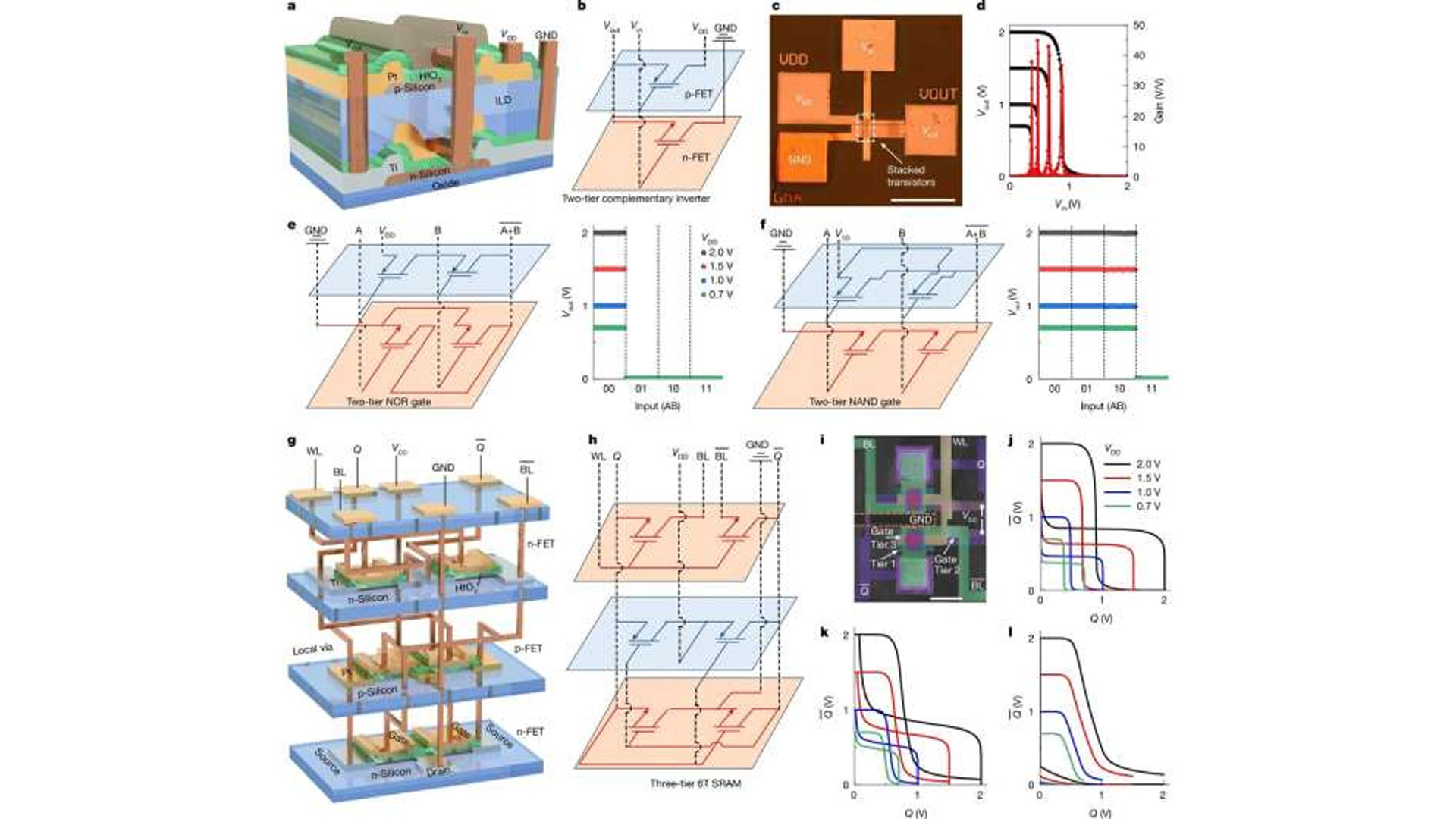
Solving the thermal crisis addresses only half the bottleneck, as engineers must physically fit more power into smaller spaces. Stacking traditional transistors requires temperatures that destroy underlying layers. Scientists at the University of Illinois circumvented this utilizing flexible silicon sheets merely ten nanometers thick. These ultra-thin layers are applied using a specialized roller safely below two hundred degrees Celsius. This innovative technique allows for dense vertical stacking without melting the circuitry below.
• Vertical stacking normally destroys underlying circuitry.
• Engineers used ten-nanometer silicon sheets to build layers safely.
• The rolling technique operates below two hundred degrees Celsius.

Both experimental technologies demonstrated extraordinary reliability during rigorous laboratory testing. The optical switching element performed over a billion operations while maintaining total magnetic stability. The ultra-thin silicon method yielded working three-layer memory cells that drastically shrank the physical footprint. These independent achievements represent a monumental leap toward a new era of electronics. Devices could soon be vastly smaller and infinitely faster.
• The optical switch completed over a billion stable operations.
• Three-layer memory cells successfully reduced the physical footprint.
• Both technologies proved highly reliable in laboratory environments.
Transitioning these prototypes into commercial realities remains a formidable engineering challenge. Manufacturers must scale the three-dimensional silicon stacking process to accommodate industrial wafers. The light-speed processor faces supply chain hurdles, as tantalum is a highly sought-after rare metal. Scientists remain optimistic that commercial prototypes could emerge by the end of the decade despite these obstacles. Overcoming these final hurdles will fundamentally redefine global computing infrastructure.
• Scaling manufacturing processes remains a significant hurdle.
• Tantalum is a rare metal causing potential supply chain issues.
• Commercial prototypes may become available by the year 2030.
Via: Tech Xplore